join us in upcoming EVEntS

Masterclass Hub: Advanced Semiconductor Packaging Workshops
Bridge the Gap from Silicon Scaling to Next-Generation System Integration
As Moore’s Law slows, advanced packaging is the new frontier for semiconductor performance. Secure your team's competitive edge with our industry-vetted masterclass portfolio. We deliver practical, production-ready strategies covering everything from core material physics to hybrid bonding, glass substrates, and AI-driven manufacturing.


Track 2: Heterogeneous Integration & 3D Architectures
Deconstruct multi-die modular architectures, hybrid connections, and high-density stacking.
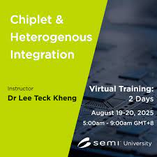
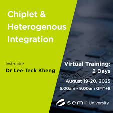
Chiplet and Heterogeneous Integration for Semiconductor packaging
Core Focus: Design methodologies for heterogeneous integration and multi-die packaging.
Advanced Package Assembly Technologies and Performance Engineering in Heterogeneous Integration
Core Focus: Performance engineering tailored specifically for heterogeneous system integration.
System-in-Package Assembly for High-Performance and Heterogeneous Integration
Core Focus: Assembly protocols for high-performance computing (HPC) nodes.
Interconnect Solutions for Chiplet and Heterogeneous Integration: Flip Chip, Thermocompression, and Hybrid Bonding
Core Focus: Comparative evaluation of Flip Chip, Thermocompression (TCB), and Hybrid Bonding.
Next-Generation 3D Packaging: 3DIC integration and TSV Technology
Core Focus: Deep dive into 3DIC vertical integration and Through-Silicon Via (TSV) physics.
Co-Packaged Optics (CPO): From Heterogeneous Semiconductor Packaging to Next-Gen Optical I/O
Core Focus: Transitioning from traditional copper to next-generation optical I/O interfaces.
Power Electronics Packaging: Thermal Management, AMB Substrates, and Sintering
Core Focus: Optimizing package architecture, advanced materials, and system performance.
Flexible Corporate Training Delivery
On-Site Technical Labs: Hands-on training tailored directly to your team's current product tape-out.
Interactive Virtual Cohorts: Live, remote masterclasses designed for geographically distributed R&D teams.
Custom Modular Curriculums: Mix and match individual modules across tracks to build your perfect syllabus.
Track 1: Packaging Foundations & Executive Strategy
Align technical roadmaps with business objectives and structural engineering fundamentals.
Semiconductor Packaging Assembly Excellence – Assembly, Material to Characterization
Core Focus: Master structural assembly, advanced material selection, and rigorous characterization.
Design and Enhancement of Package Performance
Core Focus: Design and enhance package thermal, electrical, and mechanical capabilities.
Semiconductor Packaging Substrate and Interposers: From Lead-frame, Ceramic, Organic, Silicon to Glass Substrates and Interposers
Core Focus: Comparative navigation of traditional and emerging substrate types.
From PCB, Surface Mount Technology to joint reliability: PCB, SMT, soldering and its joint reliability
Core Focus: Managing board-level metallurgy and long-term solder joint integrity.
Insight into Advanced Packaging and Trends for Business Executive
Core Focus: High-level strategic overviews of advanced packaging ecosystems and market trends.


Track 4: Substrate Fabrication, PCB & SMT Reliability
Prevent early board-level field failures through robust interfacial engineering and metallurgy.
Data-Driven Manufacturing: Unlocking Productivity with TPM, OEE Analytics and Artificial Intelligence
Core Focus: Utilizing predictive maintenance, real-time Overall Equipment Effectiveness tracking, and machine learning models for defect classification.
Insight to Industry 4.0 and AI for Manufacturing
Core Focus: Deploying smart sensor matrices, automated cyber-physical systems for deep-learning yield enhancement on the factory floor.


Track 3: Wafer, Panel & Precision Processing
Optimize high-density redistribution layers and microscopic die preparation techniques
Breaking Down Fan-out Panel & Wafer-Level Packaging: Design, Assembly, and Competitive Technologies
Core Focus: Breaking down fan-out panel and wafer-level packaging mechanics.
Wafer-Level Packaging and C4 Flip Chip Interconnects for Advanced Semiconductor Integration
Core Focus: Implementing robust wafer-level packaging and Controlled Collapse Chip Connections.
Backgrinding and Dicing in the Era of 3D IC and Advanced Packaging
Core Focus: Zero-defect wafer thinning and precision dicing for fragile 3D IC layouts.


Track 6: Smart Manufacturing, Industry 4.0 & AI for Manufacturing
Leverage Industry 4.0 data streams and artificial intelligence to optimize equipment availability, factory-wide OEE, and process yields
The BT Substrate Journey in Semiconductor Packaging: Materials, Fabrication, Assembly to Reliability
Core Focus: Navigating Bismaleimide Triazine materials, fabrication, assembly, and reliability.
Glass core substrate for advanced packaging: Material, Process and Integration
Core Focus: Practical look at glass materials, TGV processes, and system integration.
Plating Technologies and Surface Treatments for High-Reliability Packaging
Core Focus: Advanced plating technologies and high-reliability surface finish metrics.
Insight to Surface Mount Technology: Material, Process, Equipment and Quality Control
Core Focus: Deep dive into surface mount technology materials, equipment, and line quality control.
PCB Design & Electrical Performance: From Fabrication, Assembly to Embedded Passive Technologies
Core Focus: Managing electrical performance from raw fabrication to embedded passive technologies.
Track 5: Reliability Management & Failure Analysis
Diagnose, isolate, and mitigate yield-killing defects before they reach your customers.
Package Reliability Management: Failure Mechanisms, Failure Analysis and Material Characterization Techniques
Core Focus: Systematic mapping of failure mechanisms using advanced material characterization.
Corrosion & Delamination in Semiconductor Packaging: Mechanisms, Analysis, Package Enhancement
Core Focus: Root-cause analysis of package delamination and moisture-induced corrosion.
Interfacial Adhesion and Surface Finishes in Microelectronics Packaging
Core Focus: Engineering surface finishes to eliminate microelectronics interface degradation.


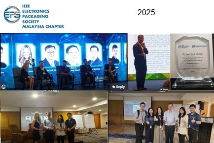
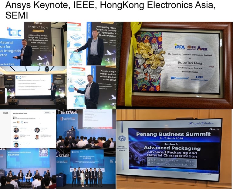
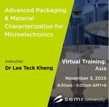
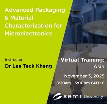
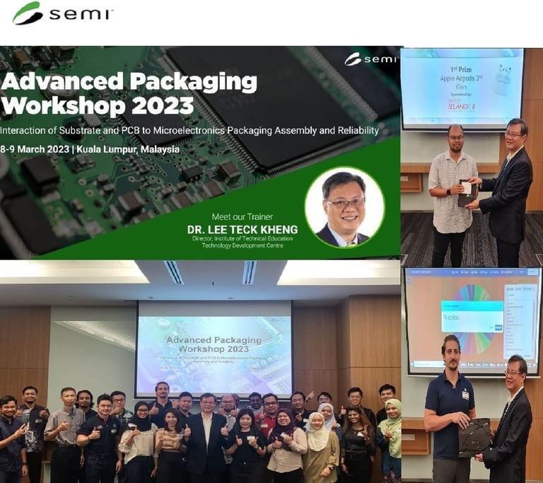
Workshop Moments
Snapshots from advanced packaging sessions.
FAQs
Who should attend?
Engineers, product developers, and industry professionals eager to learn advanced packaging.
What topics covered?
We cover hybrid bonding, glass core substrates, chiplet integration, and ecosystem building.
How long is each workshop?
Workshops typically last one to two days, combining theory with problem solving for practical learning.
Are materials provided?
Yes, all participants receive detailed notes and reference materials after the workshop.
Can workshops be customized?
Absolutely, we tailor content to your company’s specific product and innovation goals.
How do I register for a workshop?
Visit launchxtec.com, select your preferred workshop, and fill out the registration form online.