join us in upcoming EVEntS
Upcoming Workshops (Singapore)
Workshops for learning
For more details of the workshops, pls sent email to admin@launchxtec.com
Venue: Newcastle Australia Institute of Higher Education Singapore, 230 Victoria Street, #04-09/10, Bugis Junction Towers, S188024
Registration fee: SGD 800 per workshop (3 weeks before the workshop) and SGD 1,000 per workshop thereafter. We are pleased to offer the following discounts for block booking:
10% discount for registering for 3–5 workshops (any combination)
15% discount for registering for >6 workshops (any combination)
Please request a quotation by emailing admin@launchxtec.com or proceed with registration and payment via PayNow.
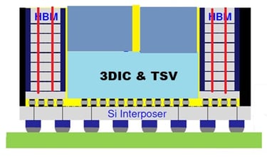
Next-Generation 3D Packaging: 3DIC integration and TSV Technology
(20-21 Aug)
This specialized program delivers a rigorous technical deep dive into the architectures, fabrication flows, and real-world deployment of 3D Integrated Circuits (3D ICs) and Through-Silicon Vias (TSVs). Attendees will master the transition from monolithic SoC design to modern multi-dimensional scaling, analyzing the structural differences, benefits, and challenges of 3D, 3.5D, and 4D packaging. By examining advanced platforms like TSMC’s SoIC alongside Wafer-to-Wafer (W2W) and Die-to-Wafer (D2W) bonding paradigms, you will gain a functional blueprint for implementing high-density silicon architectures tailored for high-performance computing, AI hardware, and next-generation memory systems.
The curriculum provides an exhaustive, step-by-step breakdown of the TSV lifecycle, exploring processing variations across Via-First, Via-Middle, and Via-Last configurations alongside critical Keep-Out Zone (KOZ) design rules. Participants will evaluate high-precision fabrication processes, comparing Deep Reactive-Ion Etching (DRIE) with laser methods, and analyzing thin-film deposition (SACVD, PECVD, ALD), barrier/seed layer formation, and bottom-up super-conformal copper plating. Finally, the workshop addresses critical back-end vulnerabilities by teaching techniques to mitigate thermal hotspot stresses, eliminate electrical voids, and apply advanced Failure Analysis (FA) to maximize production yield and package reliability.

For workshop details, pls refer to the link
https://docs.google.com/document/d/1AbYJKKeZZu98-N7FPbAXML7fViukWy7JgMLV-0ytzFE/edit?usp=sharing

For workshop details, pls refer to the link
https://drive.google.com/open?id=1N1oEjn0eCTBicOrui4uLkVglt4cGXf5o&usp=drive_fs
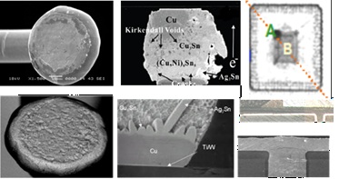
Package Reliability Management: Failure Mechanisms, Failure Analysis and Material Characterization Techniques
(17-18 Sep)
Ensure maximum semiconductor uptime and seamless qualification with our comprehensive Package Reliability Management & Failure Mechanisms Workshop. This intensive masterclass bridges the gap between material science and product longevity by providing actionable strategies to implement rigorous Design for Reliability (DFR) principles. Participants will master global compliance frameworks, including JEDEC and IEC standards, while developing a deep predictive understanding of cross-disciplinary failure modes. From evaluating thermo-mechanical stresses and physical delamination to diagnosing chemical corrosion and electrical electromigration, this module equips engineering teams with the analytical foresight needed to mitigate risks before they impact the production line.
Complementing risk management, the curriculum delivers a robust framework for physical isolation and diagnostic precision through advanced Failure Analysis (FA) and Material Characterization workflows. Attendees will gain direct insight into non-destructive testing methodologies like Scanning Acoustic Microscopy (SAM) and high-resolution imaging using SEM, EDX, and Focused Ion Beam (FIB) milling. Additionally, the program demystifies bulk thermal behaviors and interface integrity, instructing participants on how to evaluate adhesion via wire-pull and die-shear testing alongside advanced characterization tools like TGA, DSC, and DMA. Secure your asset lifecycle assurance—register today to turn complex package vulnerabilities into predictable, yield-improving outcomes.


Insight into Advanced Packaging and Trends for Business Executive
(23-24 Jul)
This Advanced Packaging Workshop is specifically designed for business executives to decode the strategic shift from traditional silicon design to the new frontier of Heterogeneous Integration. As Moore’s Law slows, the competitive edge has moved to the package, where Chiplets and 3D stacking now drive the performance gains once found only in the chip itself. This session strips away the technical jargon to focus on how architectures like CoWoS and Fan-Out are directly enabling the next generation of AI, 5G, and Automotive products while bypassing the soaring costs of monolithic chip manufacturing.
Through a commercial lens, the workshop provides critical supply chain intelligence and market-readiness insights. You will compare traditional assembly flows against modern System-in-Package (SiP) strategies to identify where value is captured and where risks reside in your roadmap. By understanding the transition to next-gen substrates and hybrid bonding, leaders will leave with the clarity needed to make high-stakes investment, sourcing, and partnership decisions in a landscape where packaging is now the primary driver of profitability and speed-to-market.
For workshop details, pls refer to the link
https://docs.google.com/document/d/18LmxC6FPL4D3TG1PxfbVemL6ThRQohRT_8lTsdwtaLU/edit?usp=sharing
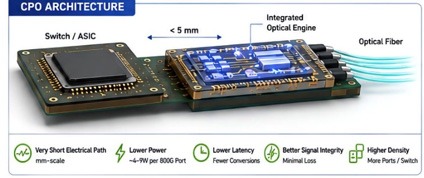
Insight to Co-packaged Optics: Hetergoeneous Integration with 3D packaging
(22-23 Oct)
Workshop synopsis in the pipeline.